Memory, Processing, & Security: Focal Points of New Automotive Releases
Automotive developers seek new ways to up safety, functionality, and comfort in modern vehicles. These mobility products may help to meet such targets.
The automotive industry is ever shifting toward electrification and autonomous driving. Electrification has inspired developers to design chips and software that optimize power management, battery performance, and charging infrastructure. Meanwhile, advanced driver assistance systems (ADAS) call for advanced hardware and algorithms that efficiently process and interpret sensor data and make real-time decisions.
This article highlights three new products released this summer from Samsung, Lattice Semiconductor, and Renesas, each designed to progress a different dimension of automotive systems.
Samsung Produces UFS 3.1 Memories for Infotainment
Universal Flash Storage (UFS), the flash storage specification for consumer electronics, bodes well in the automotive environment because of its high data transfer speeds, low latency, durability, reliability, security features, and power efficiency. As automotive systems become increasingly complex and data-driven, UFS offers important benefits for safe, efficient, and interactive driving.
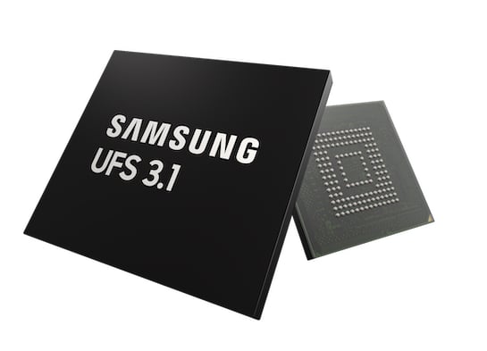
In July Samsung started mass-producing its new automotive Universal Flash Storage (UFS) 3.1 memory devices optimized for in-vehicle infotainment (IVI) systems. The new UFS 3.1 lineup offers 128, 256, and 512 GB variants.

Samsung UFS 3.1 storage devices. Image used courtesy of Samsung
Samsung reports these new products consume little power, making it easy to manage battery life efficiently. The 256 GB variant consumes 33% less energy than the previous generation of products. It also provides a sequential write speed of 700 megabytes-per-second (MB/s) and a sequential read speed of 2,000 MB/s.
Beyond automotive applications, Samsung says its new storage devices may prove useful in mobile memory solutions and 5G devices.
Lattice Rolls Out FPGA-based Drive Stack
This summer also saw Lattice Semiconductor rolling out an automotive platform, the Lattice Drive Solution, targeting several applications, including:
- In-vehicle infotainment displays
- Connectivity and data processing
- ADAS sensor bridging and processing
- Low-power zonal bridging applications for driver, cabin, and vehicle monitoring
The low-power, FPGA-based solution enables multi-resolution scaling and supports up to 4K display sizes, thanks to its video scaler IP that uses up to four different scaling algorithms. It also supports multiple displays, providing a display port interface up to 1.5x faster than similar devices. Lattice claims the solution can process data with up to 75% lower power than competing devices because it can offload the processing unit.
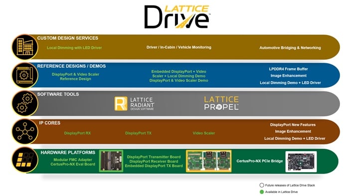
Based on the CertusPro-NX FPGA, the Lattice Drive solution stack includes the Lattice Nexus hardware platforms, IP building blocks, Lattice Radiant and Propel software design tools, reference designs, and demonstrations.

Lattice Drive solution stack. Image used courtesy of Lattice Semiconductor
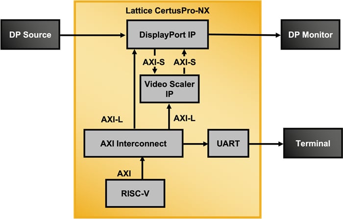
The RISC-V processor can handle video processing tasks or interact with other IP blocks for video-related functions. The AXI interconnect facilitates smooth communication between the RISC-V processor, video scaler, display port IP, and other peripherals, ensuring efficient data transfer and control flow.

Lattice Drive display port and video scaler reference design. Image used courtesy of Lattice Semiconductor
The video scaler IP resizes an input video stream to a different resolution while maintaining the aspect ratio and visual quality. The display power IP can then convert video data from the internal format of the FPGA or SoC to the display port interface's appropriate protocol. With these features, this stack enables the FPGA or SoC to process video data and output the video content to an external display through the display port interface.
Renesas Unveils Automotive Security Management
The last item in this roundup comes from Renesas, with its summer announcement of its automotive Cyber Security Management System (CSMS) for developing microcontrollers (MCUs) and systems on chips (SoCs). The TÜV Rheinland Industrie Service GmbH certified Renesas' CSMS according to International Standard ISO/SAE 21434:2021. This certification includes its 16-bit RL78 and 32-bit RH850 MCUs and the R-Car SoC family.

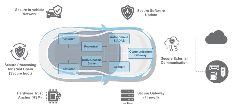
Cybersecurity applications in the automotive space. Image used courtesy of Renesas
Renesas designed the R-Car SoCs for secure external communication in autonomous vehicles. To this end, the company included hardware security modules (HSMs) to generate, safeguard, and manage cryptographic keys and execute cryptographic operations within a safe environment. The RH850 32-bit MCUs also include HSM to balance performance with low power consumption. The HSMs secure in-vehicle communication between control units. With their ultra-low power consumption and hardware security features, the RL78 family of 16-bit MCUs may be particularly useful for actuator and sensor applications.
Ετικέτες:
memory,
automotive,
processors,
fpga,
samsung,
Security,
renesas,
Lattice Semiconductor,
Universal Flash Storage


